所屬科目:研究所、轉學考(插大)◆固態電子元件
(b) .(5%)
(c) (5%)
4.The common-base current gain a of an NPN BJT can be expressed as a = γaTδ where a is the emitter injection efficiency factor, aT is the base transport factor, andδ is the recombination factor. To have an a as large (close to 1) as possible, cach of these factors must be close to l as well. For these three factors, respectively, what about device design and/or operation bias must be done to make them large? (15%) If is increased, will a increase or decrease? Why? (5%)
(a) Given that the work function of the Al is slightly larger than , the electron affinity of Si, and assumed that the oxide is perfect (completely insulating, no fixed charge/interface states within the oxide and at the interface), please plot the band diagrams of the MOS capacitor when the MOS capacitor is biased at equilibrium and threshold, respectively. You have to include (vacuum level), Ec (conduction band edge), Ei (intrinsic level) , Ev (valence band edge) and EF (Fermi level) in you plots. Please also indicate on you plot the condition that the MOS structure reaches threshold. (10%)
(b) Denote the work function of Al as ΦM. If there is now fixed charges density (per unit area) (QF) at the SiO2/Si interface, write down, without derivation, the threshold voltage for the MOS capacitor. Note that you have to express the work function of Si in term of. (6%)
(c) Repeat (b), i.c., write down , for an Al/ SiO2 /n -Si structure, albeit with NA replaced by ND. Denote again the metal work function asΦM and express the work function of Si in tem of . (6%)
 阿摩線上測驗
登入
 (5%)
 .(5%)
 (5%)
 is increased, will a increase or
decrease? Why? (5%)
 , the electron affinity of Si, and assumed that the oxide is perfect (completely insulating, no fixed charge/interface states within the oxide and at the interface), please plot the band diagrams of the MOS capacitor when the MOS capacitor is biased at equilibrium and threshold, respectively. You have to include
 (vacuum level), Ec (conduction band edge), Ei (intrinsic level) , Ev (valence band edge) and EF (Fermi level) in you plots. Please also indicate on you plot the condition that the MOS structure reaches threshold. (10%)
 for the MOS capacitor. Note that you have to express the work function of Si in term of
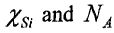 . (6%)
 , for an Al/ SiO2 /n -Si structure, albeit with NA replaced by ND. Denote again the metal work function asΦM and express the work function of Si in tem of
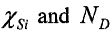 . (6%)