所屬科目:研究所、轉學考(插大)◆電子學
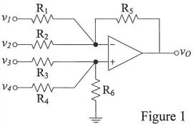
1.(20pt) Figure 1 is a summing op-amplifier to produce the output v0 = -10v1 -4v2+5v3 + 2v4・ The resistors R1 = 20 kΩ and R3 = 80 kΩ. The op-amplifier is ideal. Please determine the values of resistors R2, R4, R5 and R6. (5pt*4)
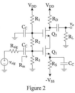
2.(30pt) For the circuit shown in Figure 2, the transistor parameters of Q1 and Q2 are: = 1.2 V, = 1.6 mA/V2, and neglect channel length modulation effect. Let R1 + R2 + R3 = 300 kΩ and Rs = 10 kΩ. = 5 V, -Vs =-5 V. (a) Please determine the R1, R2, R3 and RD such that DC current ID = 0.4 mA and DC voltage Coupling capacitor Cc is large enough that can be treated as short circuit for AC analysis. Please also find the voltage gain of small signal. (5pt*6)
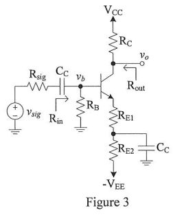
3.(25pt) The circuit configuration to be designed is shown in Figure 3 and the = -40. Assumingβ = 100, 0.7 V, and neglect Early effect. Thermal voltage VT = 26 mV. Please find the value of = 4 V and IE = 0.2 mA. And calculate the corresponding values of the AC voltage gain input resistance . Coupling capacitor Cc is large enough that can be treated as short circuit for AC analysis. (5pt*5)
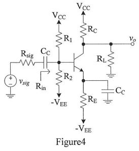
4.(25pt) For the circuit shown in Figure 4, the parameters are: = 0.1 kΩ, R1 = 40 kΩ, R2 = 5.72 kΩ, RE = 0.5 kΩ, Rc = 5 kΩ, and RL = 10 kΩ. The transistor parameters are: β = 150, 0.7 V, neglect Early effect, Cπ = 35 pF, Cμ = 4 pF, Cc= 1 μF. Thermal voltage VT = 26 mV. Please determine the lower and upper corner frequency (fL and fH), midband gain. (10pt, 10pt, 5pt)
 阿摩線上測驗
登入
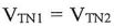 = 1.2 V,
 = 1.6 mA/V2, and neglect channel length modulation effect. Let R1 + R2 + R3 = 300 kΩ and Rs = 10 kΩ.
 = 5 V, -Vs =-5 V. (a) Please determine the R1, R2, R3 and RD such that DC current ID = 0.4 mA and DC voltage
 Coupling capacitor Cc is large enough that can be treated as short circuit for AC analysis. Please also find the voltage gain
 of small signal. (5pt*6)
 = -40. Assumingβ = 100,
 0.7 V, and neglect Early effect. Thermal voltage VT = 26 mV. Please find the value of
 = 4 V and IE = 0.2 mA. And calculate the corresponding values of the AC voltage gain
 input resistance
 . Coupling capacitor Cc is large enough that can be treated as short circuit for AC analysis. (5pt*5)
 = 0.1 kΩ, R1 = 40 kΩ, R2 = 5.72 kΩ, RE = 0.5 kΩ, Rc = 5 kΩ, and RL = 10 kΩ. The transistor parameters are: β = 150,
 0.7 V, neglect Early effect, Cπ = 35 pF, Cμ = 4 pF, Cc= 1 μF. Thermal voltage VT = 26 mV. Please determine the lower and upper corner frequency (fL and fH), midband gain
 . (10pt, 10pt, 5pt)