【系統公告】頁面上方功能列及下方資訊全面更換新版,舊用戶可再切回舊版。 前往查看

|
|
|
4.The results of a hypothetical study to measure test performance of the PCR (polymerase chain
reaction) test for Covid-19 are shown in the following table.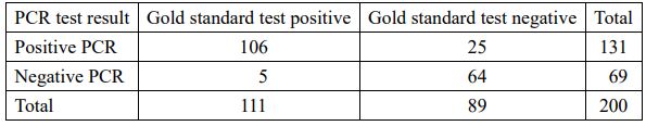
Calculate the (A) accuracy, (B) precision (positive predictive rate, PPV), (C) recall (sensitivity,
true positive rate, TPR), (D) true negative rate (TNR) and (E) F1-measure.
Note: Show the result by rounding up the 3rd digit after the decimal point, e.g. 0.9876 should be
0.988.
 VIP與詳解卡管理