 阿摩線上測驗
題組內容
6. For the digital circuit in Fig. 6, the NMOS transistor M1 is used as a pass-transistor login, which passes
logic level from Vx to VY. Assume ,and the
parasitic capacitance C = 100 fF. In consideration of the body effect, the threshold voltage of the
NMOS device can be specified as
,and the
parasitic capacitance C = 100 fF. In consideration of the body effect, the threshold voltage of the
NMOS device can be specified as 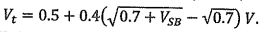
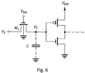
(c) Based on the charging currents in (a) and (b), please evaluate the propagation delay . [1%)