題組內容
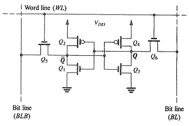
5. (25%) Design the circuit in Figure 4 to obtain a de vottage of +0.1 V at each of the drains of Q1and Q2 when . Operate all transistors at
 and assume that for the process technology in which the circuit is fabricated,
  . Neglect channel- length modulation.