所屬科目:中山◆電機◆電子學
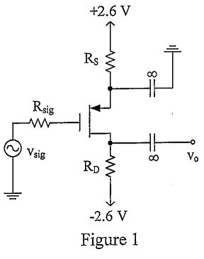
1.(20%) Figure 1 shows the CS amplifier. The threshold voltage of transistor is -0.5 V. (a) Select a value for Rs to bias the transistor at ID = 0.4 mA and IVovl = 0.4 V. Assume Vsig to have a zero DC component. (b) Select value for Ro that results in vo/vsig = -8 V/V. (c) Find the largest sinusoid Voie peak that the amplifier can handle while remaining in the saturation region. (d) If to obtain reasonably linear operation, Vsig peak is limited to 40 mV, what value can RD be increased to while maintaining saturation-region operation? (5%*4)
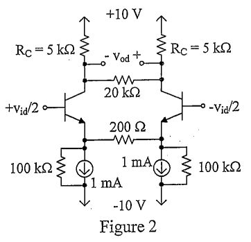
2.(20%) Figure 2 shows the differential amplifier. Please find (a) the differential gain, (b) the differential input resistance, (c) the common-mode gain assuming the resistance Rc have 2% tolerance, and (d) the common-mode input resistance. For these transistors, β = 100, thermal voltage is 25.9 mV and Early voltage VA = 100 V. (5%*4)
3. (25%) Figure 3 shows a three-stage amplifier. (a) Find the DC bias collector current in each of the three transistors and DC bias output voltage Vo. Assume IVBEl = 0.7 V, β = 100, thermal voltage is 25.9 mV and neglect the Early effect for all BJTs. (b) Find the input resistance Rin, output resistance Rout, and voltage gain vo/vi. (10%, 5%*3)
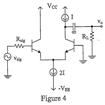
4.(20%) For the CC-CB amplifier of Figure 4, let I = 1 mA, β = 100, Cπ= 8 pF, Cμ = 3 pF,Rig = 15 kΩ, RL= 20 kΩ, and thermal voltage is 25.9 mV. Find (a) the low-frequency overall voltage gain AM, (b) the frequencies of the poles for the high frequency response, and (c) the 3-dB frequency fi. All BJIs have the same β, Cπ and Cμ. (5%, 10%, 5%)
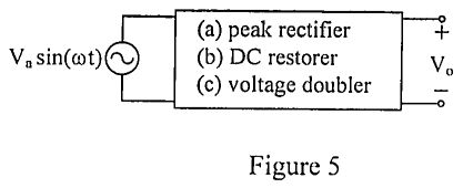
5. (15%) Please only use the diode and capacitor components to draw the circuits of peak rectifier, DC restorer and voltage doubler to come out the stable output voitage: (a) -Va, (b) -Va+ Va sin(ωt), (c) -2Va, with a stable sinusoid input voltage Va sin(ωt) as shown in Figure 5. (5%*3)
 阿摩線上測驗
登入