所屬科目:中山◆電機◆電子學
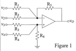
1.Figure 1 is a summing op-amplifier to produce the output . The resistors R1 = 20 kΩ and R3 = 80 kΩ. The op-amplifier is ideal. Please determine the values of resistors R2, R4, Rs and R6.
(a) Please determine the R1, R2, R3 and such that DC current = 0.4 mA and DC voltage = 2.5 V.
(b) If = 40 kΩ and R, = 2.5 kΩ. Coupling capacitor is large enough that can be treated as short circuit for AC analysis. Please also find the voltage gain and input resistance of small signal.
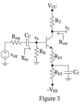
3.The circuit configuration to be designed is shown in Figure 3 and the = -40. Assuming β = 100, = 5 V, - = -5 V, = 10 kS, = 100 kΩ, 0.7 V, and neglect Early effect. Thermal voltage = 26 mV. Please find the value of to achieve DC voltage = 4 V and = 0.2 mA. And calculate the corresponding values of the AC voltage gain , input resistance . Coupling capacitor is large enough that can be treated as short circuit for AC analysis.
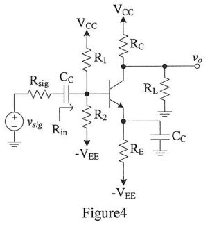
4.For the circuit shown in Figure 4, the parameters are: = 5 V, - = -5 V, = 0.1 kΩ,R1=40kΩ.R2=5.72 kΩ, = 0.5 kΩ, = 5 kΩ, and = 10 kΩ. The transistor parameters are: β = 150, 0.7 V, neglect Early effect, = 35 pF, = 4 pF, = 1 HF. Thermal voltage = 26 mV. Please determine the lower and upper corner frequency (), midband gain .
 阿摩線上測驗
登入
 . The resistors R1 = 20 kΩ and R3 = 80 kΩ. The op-amplifier is ideal. Please determine the values of resistors R2, R4, Rs and R6.
 such that DC current
 = 0.4 mA and DC voltage
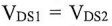 = 2.5 V.
 = 40 kΩ and R, = 2.5 kΩ. Coupling capacitor
 is large enough that can be treated as short circuit for AC analysis. Please also find the voltage gain
 and input resistance
 of small signal.
 = -40. Assuming β = 100,
 = 5 V, -
 = -5 V,
 = 10 kS,
 = 100 kΩ,
 0.7 V, and neglect Early effect. Thermal voltage
 = 26 mV. Please find the value of
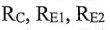 to achieve DC voltage
 = 4 V and
 = 0.2 mA. And calculate the corresponding values of the AC voltage gain
 , input resistance
 . Coupling capacitor
 is large enough that can be treated as short circuit for AC analysis.
 = 5 V, -
 = -5 V,
 = 0.1 kΩ,R1=40kΩ.R2=5.72 kΩ,
 = 0.5 kΩ,
 = 5 kΩ, and
 = 10 kΩ. The transistor parameters are: β = 150,
 0.7 V, neglect Early effect,
 = 35 pF,
 = 4 pF,
 = 1 HF. Thermal voltage
 = 26 mV. Please determine the lower and upper corner frequency (
 ), midband gain
 .