所屬科目:中山◆電機◆電子學
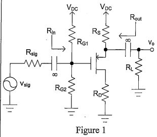
1.(20%) Figure 1 shows a MOSFET circuit with the =200 kΩ, RD = 2 kΩ, Rs = 1 kΩ, RL = 1 kΩ. The threshold voltage WIL of MOSFET are -1 V and 2 mA/V2 respectively. Neglect the channel length modulation effect. (a) Please find the DC drain current ID. (b) For AC analysis, please find the input resistance , output resistance and overall gain (5%*4)
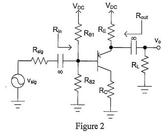
2.(20%) Figure 2 shows a BJT circuit with the = 200 kΩ, RE = 5kΩ, Rc =2 kΩ, RL= 5 kΩ. The BJT has0.7 V, β = 100, thermal voltage VT = 25 mV. Neglect the Early effect. (a) Please find the DC collector current Ic. (b) For AC analysis, please find the input resistance Rin, output resistance Rout and overall gain . (5%*4)
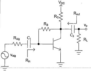
3.(30%) The amplifier shown in Fig. 3 has =RL = 1 kΩ, Rc= 1 kΩ, RB = 47 kΩ. The BJT has 0.7 V, β= 100, Cμ = 0.8 pF, fT = 600 MHz, and thermal voltage VT = 25 mV. Assume the coupling capacitors to be very large. Neglect the Early effect. (a) Find the collector current of the transistor. (b) Find the overall gain vdvsig and the input resistance at midband frequency. (c) Find the high frequency response fH. (5%,5%,10%,10%)
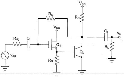
4.(30%) Consider the BiCMOS amplifier shown in Fig. 4 has= 100 kΩ, RG = 10 MΩ, Rs = 6.8 kΩ, Rc = 3kΩ, RL= 1 kΩ, CI= 0.1 μF, C2 = 1 μF. The BJT has 0.7 V, β = 200, Cμ = 0.8 pF, fT = 600 MHz, and thermal voltage VT= 25 mV. The MOSFET has = 1 V, = 2 mA/V2, and= 1 pF. Neglect the Early effect and channel length modulation effect. (a) Consider the DC bias circuit. Neglect the base current of Q2 in determining the current in Q1. Find the DC drain current in Q1 and collector current in Q2. (b) Consider the circuit at low frequencies. Deternine the frequency of the poles due to C1 and C2. (c) Consider the circuit at higher frequencies. Use open-circuit time constants to estimate fH. (5%,5%,5%,5%,10%)
 阿摩線上測驗
登入
 =200 kΩ, RD = 2 kΩ, Rs = 1 kΩ, RL = 1 kΩ. The threshold voltage
 WIL of MOSFET are -1 V and 2 mA/V2 respectively. Neglect the channel length modulation effect. (a) Please find the DC drain current ID. (b) For AC analysis, please find the input resistance
 , output resistance
 and overall gain
 (5%*4)
 = 200 kΩ, RE = 5kΩ, Rc =2 kΩ, RL= 5 kΩ. The BJT has
 0.7 V, β = 100, thermal voltage VT = 25 mV. Neglect the Early effect. (a) Please find the DC collector current Ic. (b) For AC analysis, please find the input resistance Rin, output resistance Rout and overall gain
 . (5%*4)
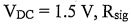 =RL = 1 kΩ, Rc= 1 kΩ, RB = 47 kΩ. The BJT has
 0.7 V, β= 100, Cμ = 0.8 pF, fT = 600 MHz, and thermal voltage VT = 25 mV. Assume the coupling capacitors to be very large. Neglect the Early effect. (a) Find the collector current of the transistor. (b) Find the overall gain vdvsig and the input resistance
 at midband frequency. (c) Find the high frequency response fH. (5%,5%,10%,10%)
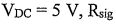 = 100 kΩ, RG = 10 MΩ, Rs = 6.8 kΩ, Rc = 3kΩ, RL= 1 kΩ, CI= 0.1 μF, C2 = 1 μF. The BJT has
 0.7 V, β = 200, Cμ = 0.8 pF, fT = 600 MHz, and thermal voltage VT= 25 mV. The MOSFET has
 = 1 V,
 = 2 mA/V2, and
 = 1 pF. Neglect the Early effect and channel length modulation effect. (a) Consider the DC bias circuit. Neglect the base current of Q2 in determining the current in Q1. Find the DC drain current in Q1 and collector current in Q2. (b) Consider the circuit at low frequencies. Deternine the frequency of the poles due to C1 and C2. (c) Consider the circuit at higher frequencies. Use open-circuit time constants to estimate fH. (5%,5%,5%,5%,10%)